XiangShan
RISC-V ecosystemXiangShan is a high-performance out-of-order RV64 core written in Chisel, started in 2019 at the Institute of Computing Technology of the Chinese Academy of Sciences. Its generations take lake names, from Yanqihu, taped out in 2021, to Nanhu and Kunminghu.
Overview
| Specification | Value |
|---|---|
| ISA support | Yanqihu: RV64GC, Nanhu: RV64GCBK |
| Microarchitecture | Out-of-order, multi-issue; generations are Yanqihu, Nanhu and Kunminghu |
| Performance density | 5.3 CoreMark/MHz at 1.3 GHz (Yanqihu) |
| Resource footprint | ASIC-oriented; the project publishes no FPGA LUT count |
| Clock domain | 1.3 GHz on 28 nm (Yanqihu), 2 GHz on 14 nm (Nanhu, 2023 tape-out) |
XiangShan is an open-source, high-performance RISC-V processor implementing the 64-bit instruction set architecture. Its cores employ out-of-order execution, allowing instructions to be processed in an order different from their original program sequence. This approach enables the processor to exploit instruction-level parallelism by executing independent operations while other instructions are waiting for their dependencies to be resolved. The hardware is described in Chisel, a hardware construction language built on Scala, and distributed under the Mulan Permissive Software License, Version 2.
The name is Chinese for Fragrant Hills, a park in western Beijing, and each generation of the design takes the name of a lake. The first generation, Yanqihu, was taped out in 2021 on a 28 nanometer process and ran at 1.3 GHz, achieving 5.3 CoreMark/MHz. Taping out means sending a finished design to a factory for manufacturing. Nanhu is the second generation, taped out in 2023 on 14 nm at 2 GHz with RV64GCBK. Kunminghu, the third, is in active development.
Microarchitecture

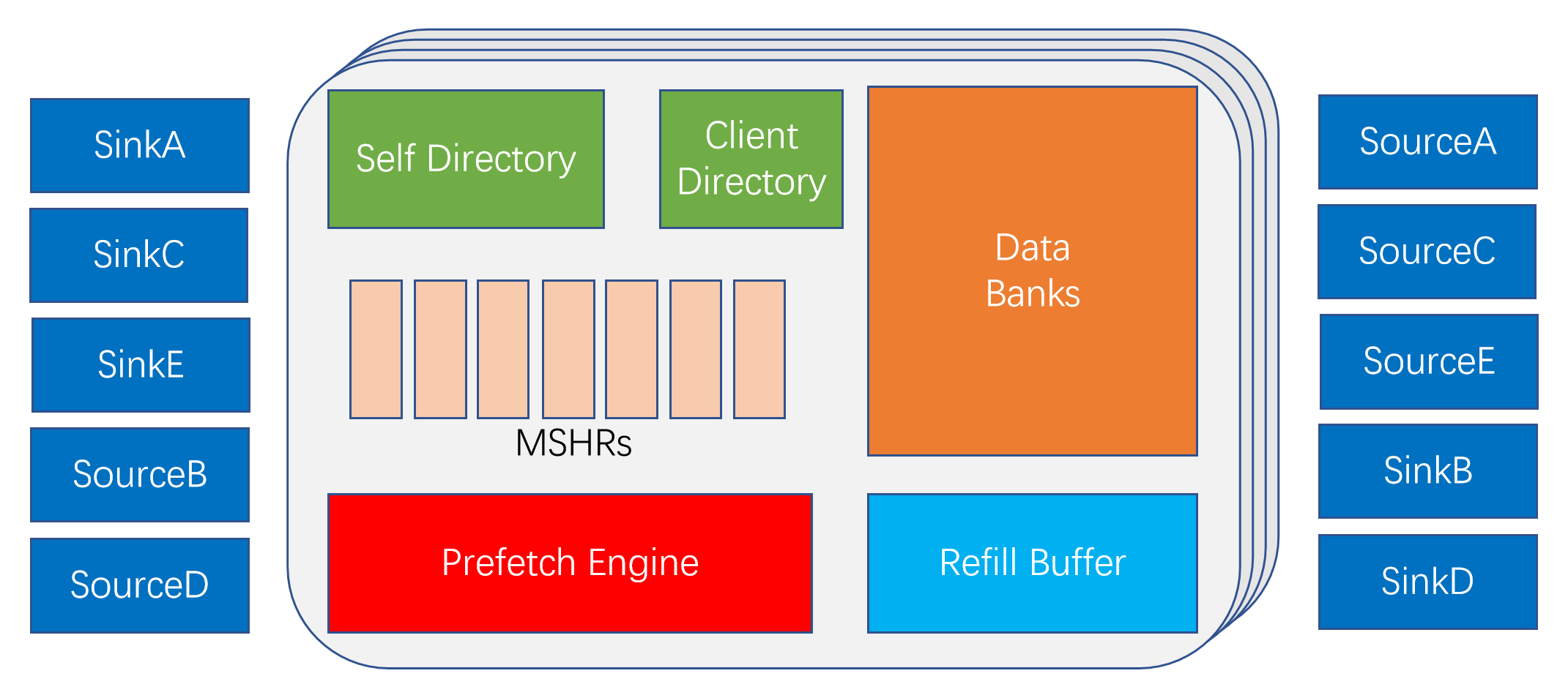
XiangShan employs an out-of-order, multi-issue architecture, allowing multiple instructions to be dispatched and executed concurrently while maintaining the correct program-visible execution order. In the Nanhu generation, the memory subsystem includes two load pipelines, two store address pipelines and two store data pipelines. Its data cache supports two 64-bit read operations per cycle, providing additional bandwidth for memory-intensive workloads. Above the individual cores, Huancun provides a shared last-level cache, allowing multiple cores to access a common cache hierarchy.
Virtual memory accesses are translated through a Translation Lookaside Buffer (TLB), with an additional L2 TLB providing further translation capacity. Physical memory access permissions and attributes are checked through the Physical Memory Protection (PMP) and Physical Memory Attributes (PMA) mechanisms. Communication between the processor cores and the surrounding system is handled through the TileLink interconnect protocol.
| Part | Yanqihu | Nanhu |
|---|---|---|
| ISA | RV64GC | RV64GCBK |
| Execution | Out of order, multi-issue | Out of order, multi-issue |
| Load pipelines | Two | Two |
| Store pipelines | Two address, two data | Two address, two data |
| L1 data cache | Two 64-bit read ports, one line-width write port | Two 64-bit read ports, one line-width write port |
| Last level cache | Huancun, shared | Huancun, shared |
| Interconnect | TileLink | TileLink |
Memory and register map
XiangShan's default physical address map assigns specific address ranges to system components, including main memory, peripheral devices and reserved regions. The Physical Memory Attributes (PMA) configuration defines the permitted access properties for these regions, determining which types of operations can be performed at each address range. When software attempts to access an address outside the defined regions or performs an operation prohibited by the corresponding attributes, the processor raises an access fault. This mechanism allows the hardware to enforce the platform's physical memory layout and access restrictions.
| Region | Address range |
|---|---|
| Peripheral space | 0x0000_0000 to 0x7fff_ffff |
| DDR | 0x8000_0000 to 0xf_ffff_ffff |
| CLINT | 0x3800_0000 to 0x3800_ffff |
| Bus error unit | 0x3801_0000 to 0x3801_ffff |
| Debug module | 0x3802_0000 to 0x3802_0fff |
| L3 cache control | 0x3900_0000 to 0x3900_0fff |
| PLIC | 0x3c00_0000 to 0x3fff_ffff |
The Platform-Level Interrupt Controller (PLIC) receives external interrupt requests through sources 1-64. Sources 65 and 66 are reserved for bus error interrupts generated by core 0 and core 1, respectively.
Physical implementation
XiangShan has progressed beyond prototyping into physical silicon implementation. Its first-generation design, Yanqihu, completed tape-out in 2021 using a 28 nm manufacturing process, with a reported operating frequency of 1.3 GHz and 5.3 CoreMark/MHz. The second generation, Nanhu, was taped out in 2023 on a 14 nm process at 2 GHz. Subsequent generations have pursued more advanced semiconductor process nodes and higher operating frequencies, reflecting the project's continued development toward increasingly capable processor implementations.
| Generation | Reported figure |
|---|---|
| Yanqihu | 28 nm, 1.3 GHz, 5.3 CoreMark/MHz, taped out in 2021 |
| Nanhu | 14 nm, 2 GHz, taped out in 2023 |
| Kunminghu | In development at the time of writing |
| FPGA | No LUT count published for the core |
Identifying the part
XiangShan is an open-source processor design that can be integrated into different SoC implementations. Identifying a XiangShan-based system requires examining the hardware platform rather than relying on a generic processor identifier. Start with the board documentation, SoC specifications or chip markings to identify the underlying implementation. If the system is accessible, inspect its boot logs, device tree and hardware description for processor information, including the ISA, core count, cache configuration and vendor-specific identifiers. The reported mvendorid, marchid and mimpid CSRs can also help identify the implementation, provided the platform exposes meaningful values for them.
The memory map places the debug module and the cache controllers at fixed addresses, which identify the platform.
| Where it appears | How to confirm |
|---|---|
| Yanqihu and Nanhu boards | Platform documentation and the fixed peripheral map |
| Research systems | Project papers and release notes |
| Software images | Device tree and the debug module base address |
Disassembly and debugging
The debug module follows RISC-V External Debug Support 0.13.2 and sits at a fixed address in the peripheral space. OpenOCD connects to it over a remote bitbang connection by default.
adapter driver remote_bitbang
remote_bitbang host localhost
remote_bitbang port 23334
jtag newtap $_CHIPNAME cpu -irlen 5| Item | Value |
|---|---|
| ISA | Yanqihu: RV64GC, Nanhu: RV64GCBK |
| Compiler flags | -march=rv64gc -mabi=lp64d for Yanqihu; -march=rv64gcbk -mabi=lp64d for Nanhu, add extensions the build enables |
| Debug module | 0x3802_0000 to 0x3802_0fff, protocol 0.13.2 |
| Program buffer | 16 bytes, abstract commands use it |
| Triggers | 10 match control triggers |
| misa (0x301) | ISA and enabled extensions |
| mvendorid (0xF11) | JEDEC vendor ID, read-only |
| marchid (0xF12) | microarchitecture ID, read-only |
| mimpid (0xF13) | implementation version, read-only |
| mhartid (0xF14) | hart that runs the code, read-only |
History
The Institute of Computing Technology of the Chinese Academy of Sciences started XiangShan in 2019, and work on the first generation began in June 2020. Peng Cheng Laboratory carried out much of the physical design, the step that turns the logic into a layout a factory can produce.
The team presented its development methods at MICRO 2022, a major computer architecture conference. The Beijing Institute of Open Source Chip, a nonprofit founded with industry partners, now coordinates development.
Where it is used
XiangShan targets the performance of commercial application processors, the kind found in phones and servers. Researchers use it to study high-end processor design, and the project publishes its simulation, verification and performance analysis tools alongside the core.