PicoRV32
RISC-V ecosystemPicoRV32 is an RV32IMC core written in Verilog and built to use as little FPGA area as possible. Claire Wolf, author of the Yosys synthesis suite, wrote it, and it often serves as a helper processor inside larger chips.
Overview
| Specification | Value |
|---|---|
| ISA support | RV32IMC, RV32E |
| Microarchitecture | Non-pipelined, multi-cycle state machine without hazard logic or branch prediction |
| Performance density | 0.516 DMIPS/MHz (4.10 CPI) with look-ahead; 0.305 DMIPS/MHz (5.23 CPI) without |
| Resource footprint | 750–2,000 LUTs on Xilinx 7-Series FPGAs |
| Clock domain | 250–450 MHz on 7-Series FPGAs; up to 769 MHz on Kintex UltraScale+ |
PicoRV32 is a size-optimized, non-pipelined 32-bit RISC-V CPU written in Verilog (ISC license), a language for describing hardware. A core is the part of a chip that executes instructions. It implements RV32IMC, the 32-bit base instruction set with multiplication and compressed instructions, and can be reduced to RV32E, a version with fewer registers. Designed primarily as a compact auxiliary control core for FPGAs and ASICs, PicoRV32 prioritizes minimal logic gate count and maximum operational frequency over single-cycle instruction execution.
Microarchitecture
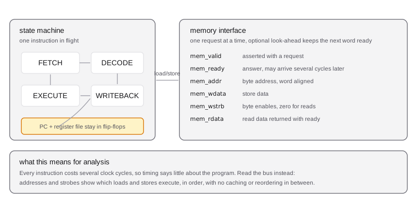
PicoRV32 uses a state-machine-driven execution core, where instruction processing is controlled by a finite-state machine (FSM) that coordinates the individual stages of execution. Unlike pipelined processors, which overlap the execution of multiple instructions, PicoRV32 processes instructions sequentially through states such as instruction fetch, decoding, execution, memory access and register writeback. Each state determines the operations performed during a clock cycle and the conditions required to advance to the next one.
This sequential execution model simplifies the processor's control logic by eliminating the need for complex register hazard detection, data forwarding networks and branch prediction mechanisms. The FSM instead manages instruction sequencing and resource access, reducing hardware requirements at the cost of instruction throughput, since multiple clock cycles may be needed to complete a single instruction.
Memory is accessed through a valid and ready handshake, where the core asserts mem_valid with an address and waits for mem_ready before completing the transaction. An optional look-ahead interface allows the next memory address to be presented in advance, potentially reducing access latency. Published DMIPS figures therefore vary between implementations with and without this feature. Interrupts do not follow the standard RISC-V trap flow. The core saves and restores its q registers with the custom getq, setq and retirq instructions, so firmware that expects mcause, mepc and standard trap handling will not run unmodified. Counter reads are implemented through rdcycle, rdtime and rdinstret when counters are enabled, which is the default, and the core exposes no other CSRs.
| Part | PicoRV32 |
|---|---|
| Execution | Multi-cycle state machine, no pipeline |
| Instructions in flight | One |
| Memory interface | mem_valid and mem_ready handshake |
| Look-ahead | Optional, improves instruction fetch |
| Interrupts | Maskable IRQ, handled with the custom getq, setq and retirq instructions instead of standard traps |
| CSRs | rdcycle, rdtime and rdinstret when counters are enabled (the default); no other CSRs |
Memory and register map
The address map belongs to the system. The core exposes a bus and a reset vector parameter, and the system decides the map. PicoSoC is one example, with the map below.
| Address | Region |
|---|---|
| 0x00000000 | Internal RAM, 256 words by default |
| 0x00000400 to 0x01ffffff | SPI flash, executed in place |
| 0x02000000 | SPI flash controller configuration |
| 0x02000004 | UART divisor |
| 0x02000008 | UART data |
PicoSoC resets to 0x00100000, inside the flash region, and takes interrupts at 0x00000000. Both are parameters of the top level, so a different build can move them.
Physical implementation
PicoRV32 targets FPGAs and is measured in lookup tables. The cited range is 750 to 2,000 LUTs on Xilinx 7-Series depending on enabled extensions and register file ports, and the quoted clock range is 250 to 450 MHz on the same family.
| Metric | Value |
|---|---|
| FPGA area | 750 to 2,000 LUTs on Xilinx 7-Series |
| Clock | 250 to 450 MHz on 7-Series, up to 769 MHz on Kintex UltraScale+ speed grade -3 |
| Process node | Not applicable, the core is synthesized into whatever FPGA or ASIC is used |
| Typical board | iCE40 boards running PicoSoC |
Identifying the part
PicoRV32 is implemented as configurable FPGA logic rather than a standalone physical processor. Its presence and configuration are determined by the FPGA design, which defines the processor core, its bus connections, memory layout and reset vector. These details can be examined through the hardware description, synthesis outputs and FPGA bitstream.
| Where it appears | How to confirm |
|---|---|
| iCE40 boards with PicoSoC | Board documentation and the flash image layout |
| FPGA designs using Yosys | Synthesis report showing picorv32 in the netlist |
| Custom SoCs | Memory map and reset vector in the top level |
Disassembly and debugging
The ISA string in the firmware attributes records whether the build has the compressed and multiply extensions, and RV32E halves the register count and changes the ABI.
riscv32-unknown-elf-readelf -A firmware.elf
riscv32-unknown-elf-objdump -d -M no-aliases firmware.elf

# firmware extraction from a PicoSoC flash image
dd if=image.bin of=firmware.bin skip=$((0x100000)) bs=1| Item | Value |
|---|---|
| ISA | RV32IMC, or RV32E with fewer registers |
| Compiler flags | -march=rv32imc -mabi=ilp32, or -march=rv32e -mabi=ilp32e |
| Debug transport | None in the core, use simulation or bus tracing |
| Reset | PROGADDR_RESET, 0x00100000 in PicoSoC |
| Interrupt vector | PROGADDR_IRQ, 0x00000000 in PicoSoC |
| CSRs | rdcycle, rdtime and rdinstret when counters are enabled; no misa or identification registers |
History
Claire Wolf, the creator of the Yosys synthesis tool, published PicoRV32 in 2015. Yosys converts hardware descriptions into circuits, and PicoRV32 became a common test design for open source FPGA tools. The repository moved to the YosysHQ organization and is now archived, and the core no longer receives active development.
Where it is used
PicoRV32 serves as an auxiliary processor, a helper core that runs control tasks inside a larger FPGA design or chip. Its high clock speed lets it join existing designs at their own clock rate. PicoSoC, an example system included in the repository, runs PicoRV32 on low-cost iCE40 FPGA boards.